Design A Combinational Circuit With Four Inputs

4 Bit Parallel Subtractor Parallel Logic Design

Combinational Logic Logic Electronic Engineering Circuit

2 Bit Comparator 2 Bits Logic Digital Circuit

4 Bit Comparator Logic Electronics Circuit Bits

Logic And Gate Tutorial Truth Table Electronics Area Logic Tutorial Truth

2 Bit Synchronous Up Counter Electronics Circuit Circuit Digital
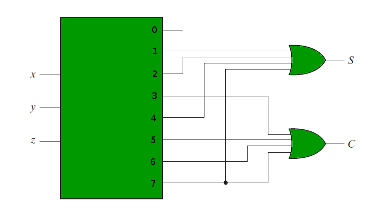
The inputs are d3 do and the output goes to the blanking input of the 7447.
Design a combinational circuit with four inputs.

Https Encrypted Tbn0 Gstatic Com Images Q Tbn 3aand9gcr6o Df7gsnnnzkgehb3dv3xn6a0 Obqerb4g Usqp Cau

Piso Shift Register Shift Register Shift Electronics Circuit

4 Bit Asynchronous Up Down Counter Counter Electronics Circuit Circuit
Combinational Circuits Using Decoder Geeksforgeeks

Pipo Shift Register Shift Register Electronics Circuit Digital
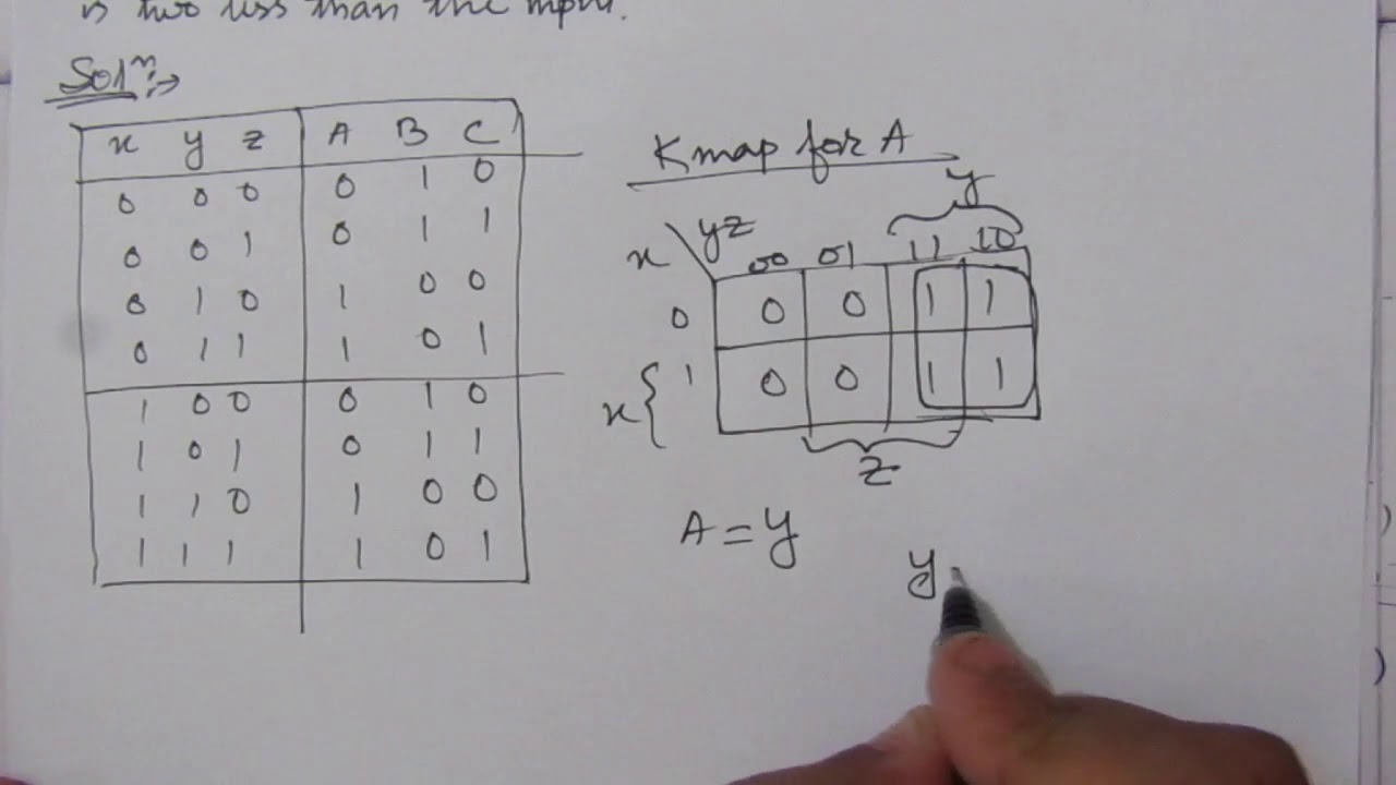
Q 4 5 Design A Combinational Circuit With Three Inputs X Y And Z And Three Outputs A B And C Youtube

Decade Counter Electronics Circuit Counter Circuit

High Voltage Low Current Power Supply 2000vdc From 15vdc High Voltage Power Supply Circuit Ups Power Supply

Lm339 Datasheet Quad Comparator How To Use Eleccircuit Com Quad Circuit Connection
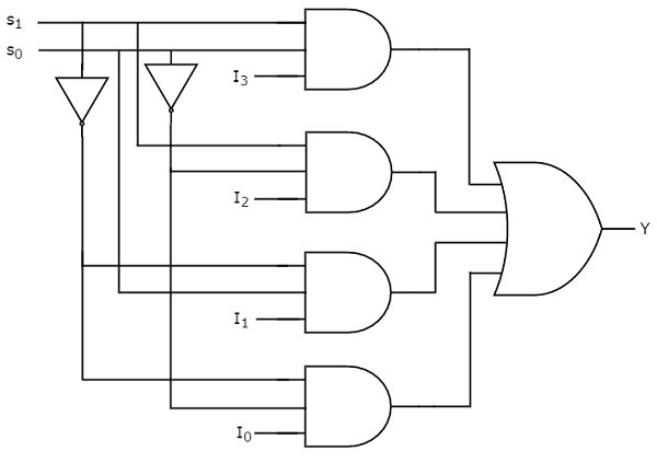
Digital Circuits Multiplexers Tutorialspoint
L04 Combinational Logic

Transimpedance Amplifier This Fast Photodiode Transimpedance Amplifier Is Based On A High Speed Jfet Input Op Amp Opa657 Circuit Simulator Circuitry Circuit

Vhdl Code For Sequence Detector 101 Using Moore State Machine And Vhdl Code For Sequence Detector 101 Using Mealy State Machine Coding Detector States

Gray To Binary Code Converter 4 Bit Coding Binary Converter

Railway Points Sequencer Electronic Schematics Electronic Circuit Projects Electronic Circuit Design
Https Ece Uwaterloo Ca Msachdev Ece223 Assignment4 Solution 3rd Edition Pdf

Binary To Gray Code Converter 3 Bit Coding Converter Binary

Carry Select Adder Vhdl Code Coding Carry On The Selection
Https Encrypted Tbn0 Gstatic Com Images Q Tbn 3aand9gctrp1c1lubgfwn7nhpfb69o1dj4hag8oge3agctusex3kh14rlx Usqp Cau

A Transistor Based Computer Circuit Electronics Circuit Transistors Circuit

Vhdl Code For Flipflop D Jk Sr T Coding Binary Code Seniors

Isolated Digital Output Module Ladder Logic Digital Plc Programming

4 Preamplifier Circuits Using Transistors Eleccircuit Com Transistors Electronic Circuit Projects Circuit
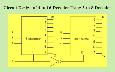
How To Design A 4 To 16 Decoder Using 3 To 8 Decoder
Source : pinterest.com
