Design Combinational Circuit Three Inputs

Three Input Circuit With Redundant Gates Simple Circuit Algebra Equations Some Text
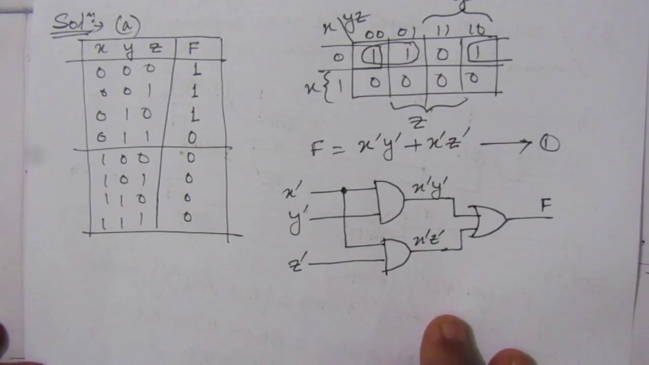
Q 4 4 Design A Combinational Circuit With Three Inputs And One Output A The Output Is 1 When Youtube
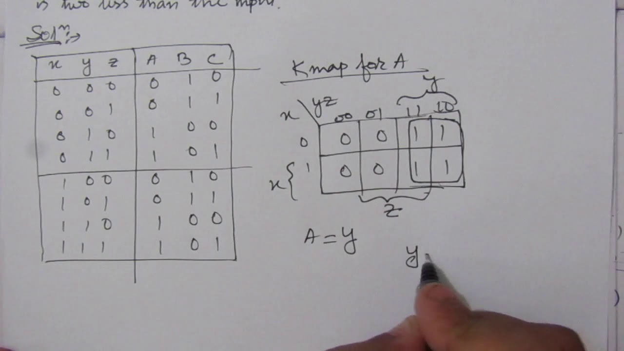
Q 4 5 Design A Combinational Circuit With Three Inputs X Y And Z And Three Outputs A B And C Youtube

Pin On Digital Logic Circuits

Combinational Logic Circuits Functions And Classification Circuit Electronics Projects Logic
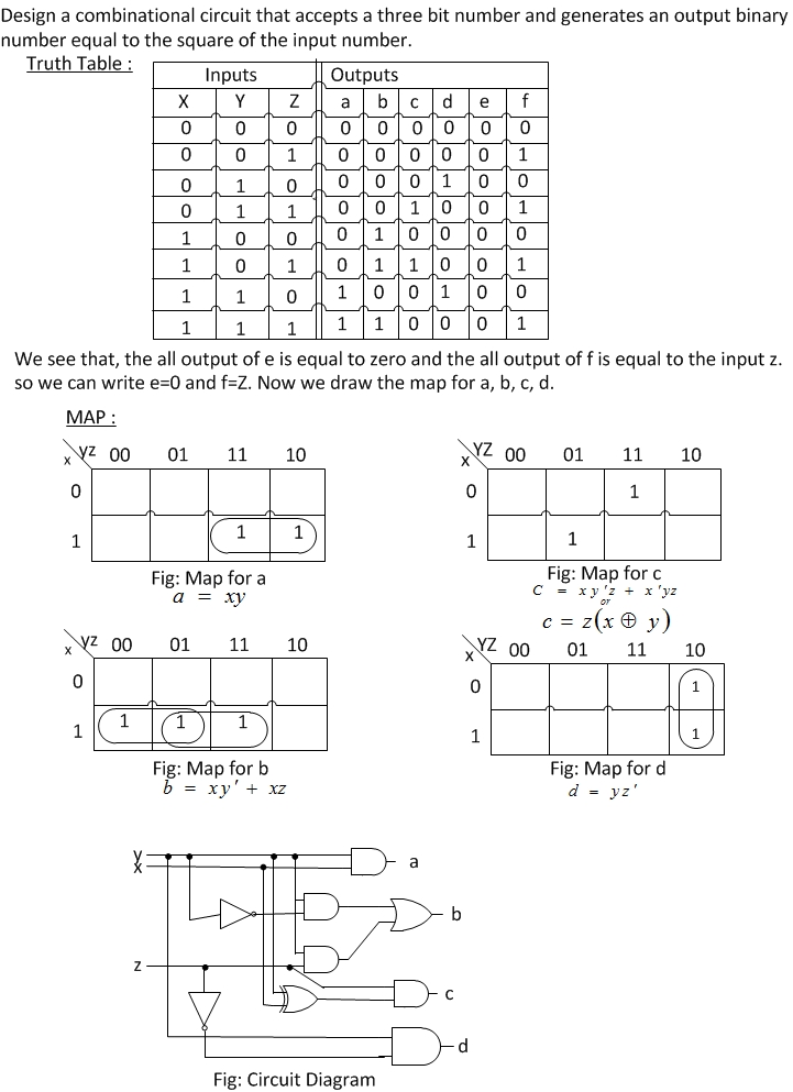
Logic Circuit Of Square Of 3 Input Variable Sukanta S Diary

The design procedure for combinational logic circuits starts with the problem specification and comprises the following steps.
Design combinational circuit three inputs.

Design Of Parallel Adder In 2020 Binary Number Parallel Simple Solutions
Https Ece Uwaterloo Ca Msachdev Ece223 Assignment4 Solution 3rd Edition Pdf

1 Bit Comparator Logic Electronics Circuit Bits

2 Bit Synchronous Up Counter Electronics Circuit Circuit Digital
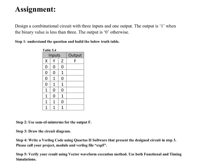
Solved Assignment Design A Combinational Circuit With Th Chegg Com

Combinational Circuits Circuit Electronics Circuit Block Diagram

Combinational Logic Circuits 3 Logic What Is Meant Circuit
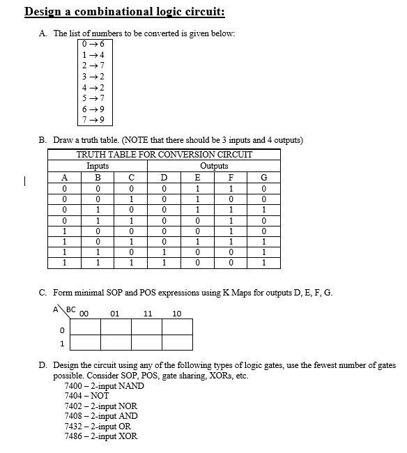
Solved Design A Combinational Logic Circuit The List Of Chegg Com

3 Bit Synchronous Up Down Counter Electronics Circuit Counter Circuit

Logic And Gate Tutorial Truth Table Electronics Area Logic Tutorial Truth

Pin On Electrical

Pin On Mrmgate

Combinational Circuit Using Logic Gates Digital Electronics Electronics Area Circuit Logic Electronics

Combinational Logic Logic Electronic Engineering Circuit

Binary To Gray Code Converter 3 Bit Coding Converter Binary

Multiplexers Using Logic Gates Circuit Design Electronics Circuit Circuit

4 Bit Parallel Subtractor Parallel Logic Design

4 Bit Comparator Logic Electronics Circuit Bits
Https Encrypted Tbn0 Gstatic Com Images Q Tbn 3aand9gctwfpfbf0ekbpk63pq8e9jykh7z6h5ez0q Radxdse88hiwcusz Usqp Cau

Gray To Binary Code Converter 4 Bit Coding Binary Converter

Logic Gates Symbols Electronic Engineering Electronics Basics Electricity

3 Best Transformerless Inverter Circuits Homemade Circuit Projects Electronic Circuit Projects Circuit Projects Circuit Design

Digital Logic Gates Using Nand Gates Electronics Electrical Circuit Design Digital Electronics
Simulation Of A Half Adder Circuit With 4 Basic Gates Using Tina Circuit Design Simulation Circuit Simulator
Source : pinterest.com
